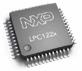
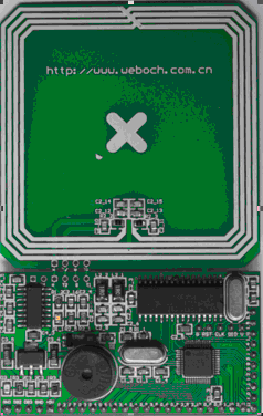
Cortex-M0 LPC1200系列微控制器
Powered by the smallest, most energy-efficient Cortex-M0 core, the LPC1200 provides compelling solutions for industrial control. The series includes up to 128 KB Flash and 8 KB SRAM, and offers configurable peripherals ideally suited for energy-efficient controls and appliances.
基于低功耗的Cortex-M0內核,LPC1200系列為工業控制提供了強有力的解決方案。該系列產品包 含高達128KB的FLASH、8KB的SRAM,并提供了適用于低功耗控制和應用的可配置外設。

Key features:
- * ARM Cortex-M0 processor
- Up to 30 MHz CPU frequency with zero wait state from Flash
- Nested Vectored Interrupt Controller (NVIC) supports ` 32 vectored interrupts with fast and deterministic latency
- Three reduced-power modes: Sleep, Deep-sleep, and Deep power-down
- * Memories
- Up to 8 kB SRAM
- Up to 128 kB Flash memory with 512 Byte page eraseSerial communication interfaces
- * Serial communication interfaces
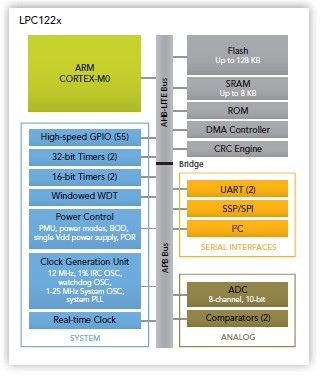
- Two UARTs with fractional baud-rate generation and internal FIFO plus RS-485, modem, and IrDA supports
- I2C with Fast-mode Plus for twice the devices on one bus and longer transmission distances } SSP (SPI) controller with FIFO and multi-protocol capabilities Analog peripherals
- 10-bit Analog-to-Digital Converter (ADC) with eight channels and conversion rates up to 400 ksps
- Two comparators, each with up to six selectable external sources, fully configurable on either positive or negative comparator input channels
主要特色:
- * ARM Cortex-M0處理器
- CPU頻率高達30MHz,帶有高速Flash(zero wait state)
- 嵌套向量中斷控制器(NVIC)支持32個向量中斷
- 3種省電模式:睡眠模式、深度睡眠模式、深度掉電模式(power-down)
- * 存儲器
- 高達8KB的SRAM
- 高達128KB的flash,帶有512字節的頁擦除(page erase)
- * 系列通訊接口
- 兩個UART,包含波特率生成器、內部FIFO+RS-485,lrDA
- I2C,快速模式兩倍于一條總線的速度和傳輸距離
- * SSP(SPI)控制器,支持FIFO、多種協議
- * 模擬外設
- 10位模數轉換(ADC),8通道、轉換速率高達400 ksps
- 2個比較器,每個都可選擇6個內部資源,正或負輸入通道
- * 其他外設
- DMA控制器,21通道,支持板上RART、SPI、ADC、RTC、計數器/定時器、比較器、I2C、GPIO
- 循環冗余檢查(CRC)
- 2個16位通用計數器/定時器,2輸入、2輸出
- 看門狗定時器(WDT)
- 32位實時時鐘
- 高達55個通用I/0(GPIO)

The LPC1200 series extends NXP’s 32-bit ARM microcontroller continuum by targeting a wide range of industrial applications in the areas of factory and home automation. The series offers a wide range of Flash memory sizes, from 32 to 128 KB, with 512 Bytes page erase. Benefitting from the ARM Cortex-M0 Thumb instruction set, the LPC1200 has up to 50% higher code density compared to common 8/16-bit MCUs performing typical tasks. The LPC1200 also features an optimized` ROM-based divide library for Cortex-M0, which offers code size saving and several times the arithmetic performance of software based libraries. The high efficiency of the Cortex-M0 core also helps the LPC1200 achieve lower average power for similar applications. The LPC1200 has up to 55 GPIO and new onboard peripherals including DMA, CRC, comparators, an RTC, and a 1% internal oscillator, which provides the accuracy needed for Baud rate generation.
LPC1200系列擴展了NXP(恩智浦)32位ARM微控制器的應用范圍,包括工業、家庭自動化。該系 列提供了從32到128KB的FLASH存儲器容量,帶有512KB頁擦除。得益于ARM Cortex-M0 Thumb指令 集,LPC1200比傳統的8/16位MCU高出50%代碼密度。針對Cortex-M0,LPC1200優化了ROM除法庫, 其算法性能高出軟件庫數倍。Cortex-M0內核更讓LPC1200具有更低的功耗。LPC1200有高達55個 GPIO,外設包括DMA、CRC、比較器、RTC,1%的內部振蕩器,可滿足波特率的精確需求。
LPC1200系列ARM選型表
| Type number | Product status | fmax [max] (MHz) | FLASH (kB) | RAM (kB) | I/O pins | USB device | CAN | UART | I2C | SPI | ADC | Timers | PWM | Package name | PLL | VDD [min] (V) | VDD [max] (V) | CPU supply voltage (V) |
| LPC1224FBD48 | Production | 30 | 32 | 4 | 39 | 2 | 1 | 1 | 8 | 4 | LQFP48 | Y | 3 | 3.6 | ||||
| LPC1224FBD64 | Production | 30 | 32 | 4 | 55 | 2 | 1 | 1 | 8 | 4 | LQFP64 | Y | 3 | 3.6 | ||||
| LPC1225FBD48 | Production | 30 | 64 | 8 | 39 | 2 | 1 | 1 | 8 | 4 | LQFP48 | Y | 3 | 3.6 | ||||
| LPC1225FBD64 | Production | 30 | 80 | 8 | 55 | 2 | 1 | 1 | 8 | 4 | LQFP64 | Y | 3 | 3.6 | ||||
| LPC1226FBD48 | Production | 30 | 96 | 8 | 39 | 2 | 1 | 1 | 8 | 4 | LQFP48 | Y | 3 | 3.6 | ||||
| LPC1226FBD64 | Production | 30 | 96 | 8 | 55 | 2 | 1 | 1 | 8 | 4 | LQFP64 | Y | 3 | 3.6 | ||||
| LPC1227FBD48 | Production | 30 | 128 | 8 | 39 | 2 | 1 | 1 | 8 | 4 | LQFP48 | Y | 3 | 3.6 | ||||
| LPC1227FBD64 | Production | 30 | 128 | 8 | 55 | 2 | 1 | 1 | 8 | 4 | LQFP64 | Y | 3 | 3.6 | ||||
| LPC12D27FBD100 | Production | 3.00E+07 | 0 | 8 | 40 | 2 | 1 | 1 | 8 | 4 | LQFP100 | Y | 3 | 3.6 |
Additional features:
- Programmable high-current output driver on four pins
- Processor wake-up from Deep-sleep mode via 12 port pins or peripherals interrupts
- Power-On Reset (POR)
- Brownout detect with four separate thresholds for interrupt and forced reset
- 12 MHz internal RC oscillator trimmed to 1% accuracy that can also be used as a system clock or Baud rate generatorPLL allows CPU operation up to the maximum CPU rate without the need for a high-frequency crystal. Can be run from the main oscillator, the internal RC oscillator, or the Watchdog oscillator
- Clock generation unit with divider that can reflect the main oscillator clock, IRC clock, CPU clock, and Watchdog clock.
- Available in 48- or 64-pin LQFP package
其他特色:
- 可編程控制引腳
- 可通過12引腳或外設中斷把處理器從深度睡眠中喚醒
- 上電復位
- 中斷或強制復位監測
- 12MHz內部RC振蕩器,1%精確度,可作為系統時鐘或波特率生成器
- PLL,可使CPU運行在最大CPU速率,無需高頻率晶振。可用主振蕩器、內部RC振蕩器或看門狗 振蕩器
- 時鐘產生部件可影響主振蕩器時鐘、IRC時鐘、CPU時鐘、看門狗時鐘
- 48或64引腳封裝


